
Photonic Crystals
Optics and photonics are the future of new tech, but how do we get there?

In April, IEEE’s flagship magazine Spectrum included an article on high-powered lasers and the key technology behind what makes them achieve efficiencies far greater than today’s lasers: photonic crystals.
First, hats off to the authors for a very well-written and easy to understand article, albeit the audience is engineers. I encourage you to read it.
Second, these giant leaps in technology are being powered by the next game-changer in engineering: Nanophotonics.
Magic, tiny air holes.
Photonic crystals. What a name! This magic-sounding technology is representative of the next wave of optics, slightly more dull than the name conjures in your mind (photons! crystals! it has it all! quick, to the nearest metaphysical science-fairy ring!).
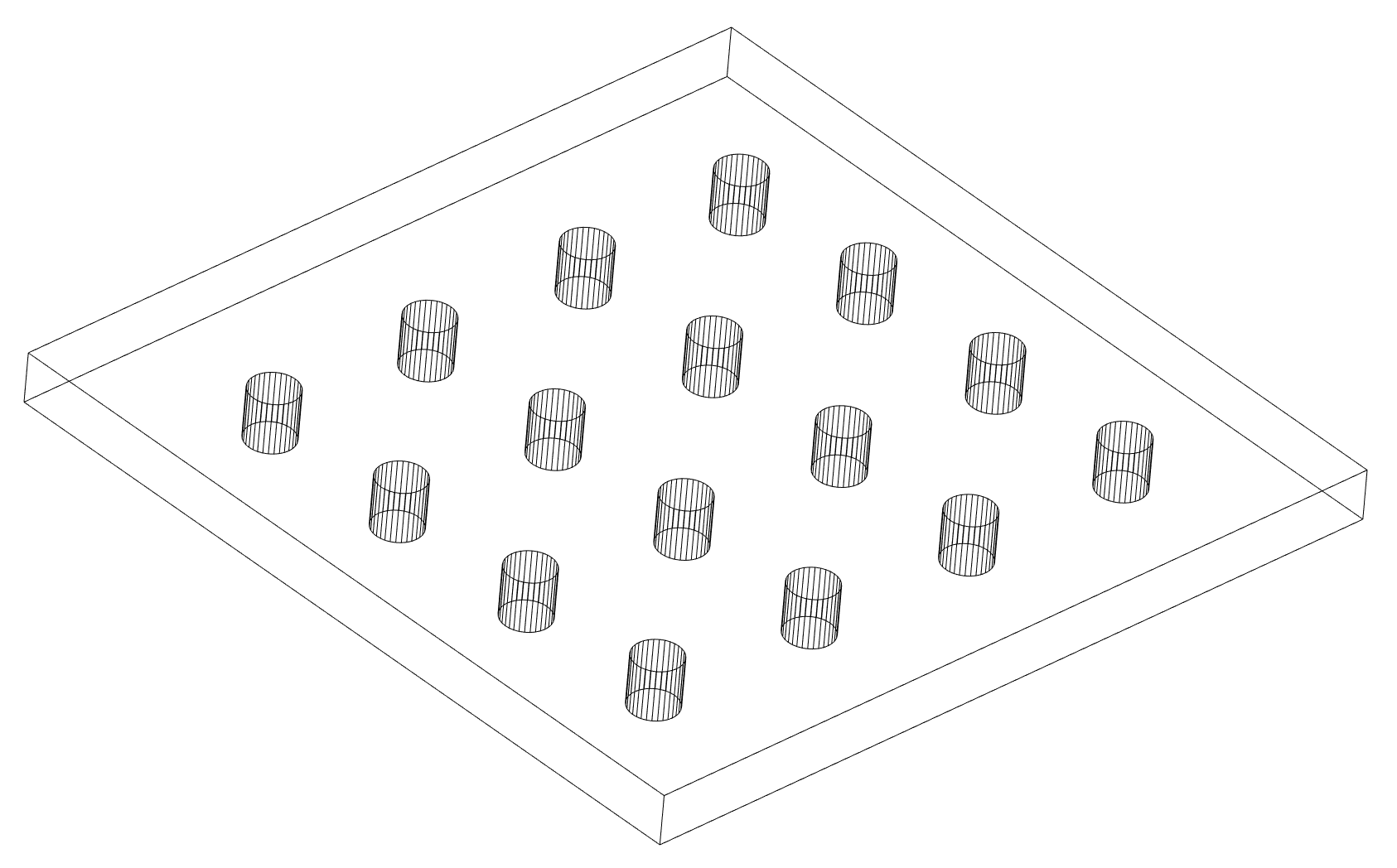
A photonic crystal is a material with tiny ‘holes’ evenly spaced in tiny increments. Very, very tiny holes at very, very tiny increments - nanometer-scale. These holes are disruptions in the refractive index of the surrounding material.
Disruptions create reflection and bending of light - think about sunlight both reflecting off of a lake and bending to make a fish look like it’s in a different spot than it actually is. Each hole partially reflects and partially bends the incoming light, which causes the next hole to partially reflect and partially bend the light, and so on and so on.
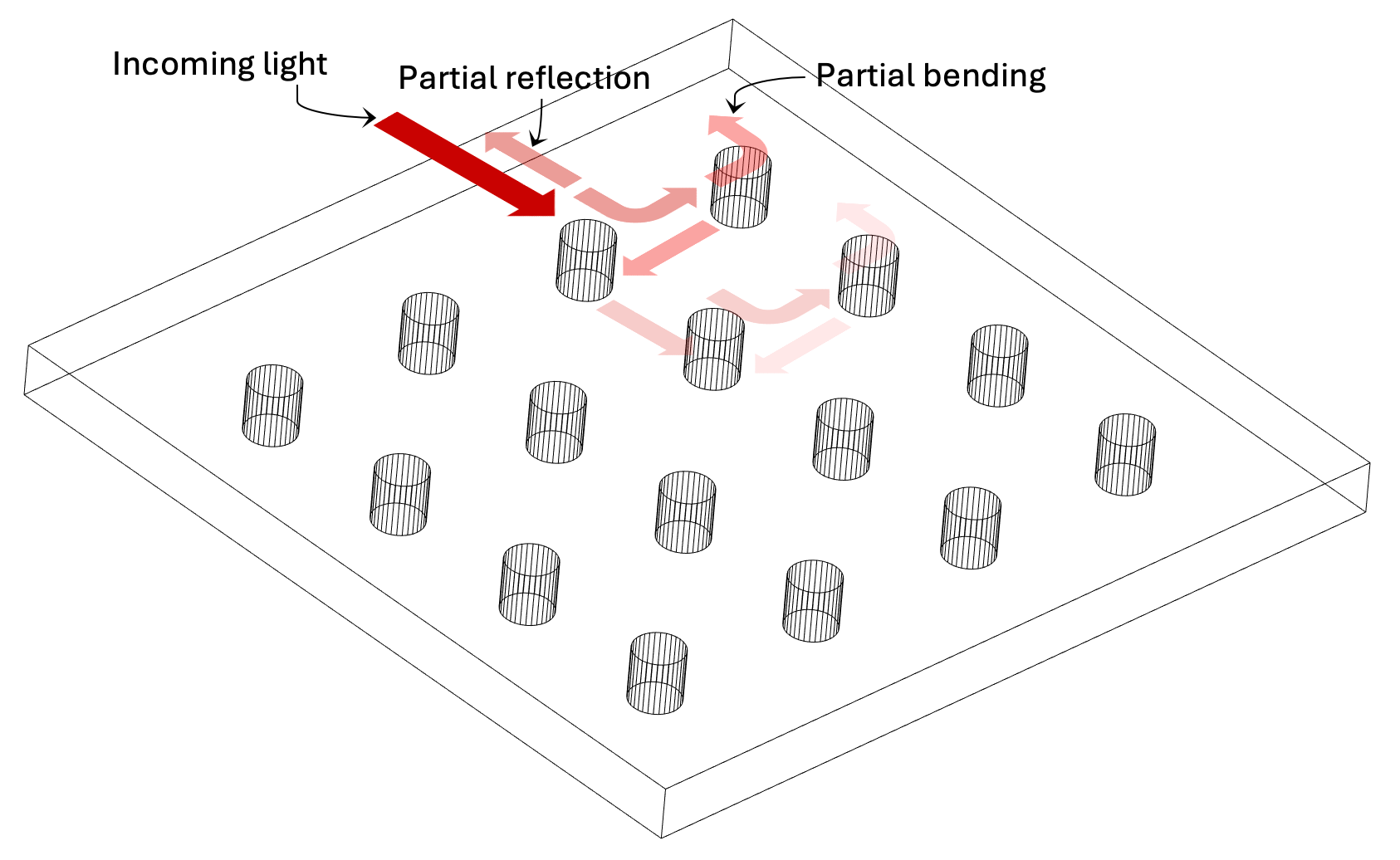
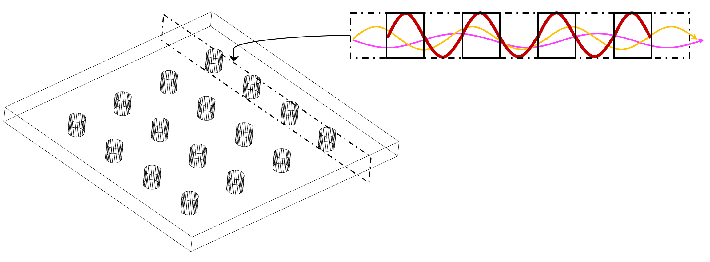
Just the right size and shape of these holes placed at just the right increment will create reflections and bends that result in standing waves - a particular wavelength of light that does not move through the material, whereas all other wavelengths move on through.
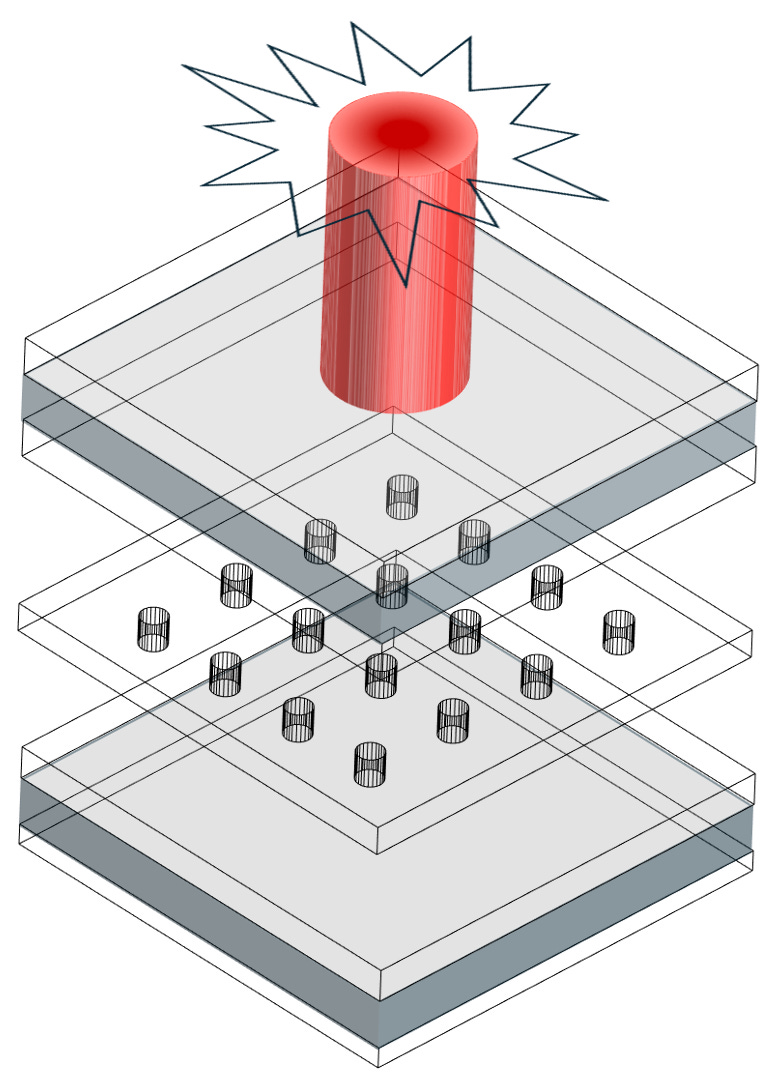
Sandwiching a photonic crystal layer into a laser structure allows a two-dimensional standing wave to form from the light-generating active layer, which then amplifies the standing wave. The result is a high quality, broad circular beam emitting from the surface of the laser (as opposed to the elliptical shape of an edge-emitting laser).
Et voilà, the PCSEL (Photonic Crystal Surface Emitting Laser)! An incredibly high brightness, high efficiency, compact laser with scalability far beyond current laser technology.
Manipulations of the holes - for example, triangle-shaped holes or two overlapping patterns of different-sized holes - can further enhance the efficiency of the laser by cancelling undesirable higher-order modes and narrowing divergence (the way the beam spreads out as it leaves the device).
So, who cares?
What does a high-efficiency, low-divergence laser mean, exactly? Small lasers that can cut steel, directed energy weapons (laser guns!), light propulsion for space probes, better telecommunications tech, and compact lidar (sensors used for self-driving vehicles) without lenses.
And all of this paradigm shift is being propelled by a tiny little optical device.
Basically, there are huge implications in these tiny air holes.
Technology realization like this also showcases the expanding utility of the semiconductor foundry. We are entering a phase in industrial-level technology where we can control the nanoscale in mass production.
That’s wild, space-age stuff.
What’s next?
Some background on me: my research field of interest is in how periodic structures can manipulate optical properties. That is, how tiny little repeating patterns in a material can change light.
Metalenses, for example, utilize pillars instead of the holes of photonic crystals and are poised to upend traditional optics by replacing round lenses with thin, flat ones.
That’s right, a flat optic.
Have thick eyeglasses? Slap a metalens in a frame and you’ll be crewing it up with the cool kids.
Tired of lugging around that heavy 20x rifle scope? Get the new and improved version with 1/10th the weight and 1/100th the glare.
We have been stuck with large, bulky optics for hundreds of years. Like Large Language Models (LLMs) and image generators did last year, nanophotonics will be the sneaky revolution around the corner that upends the game.
Cheaper, faster, better. Get rid of the bulky, heavy, expensive components. Sense more properties with less energy.
Magic!
Impressive, and well-explained.
Amazing stuff. Also scary. Thanks